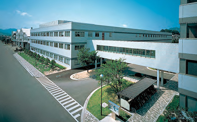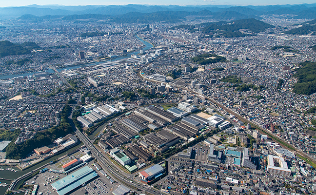
Industrial machinery business
Supports higher quality and efficiency in electronic device production
Providing consistent solutions from manufacturing and sales to maintenance services.
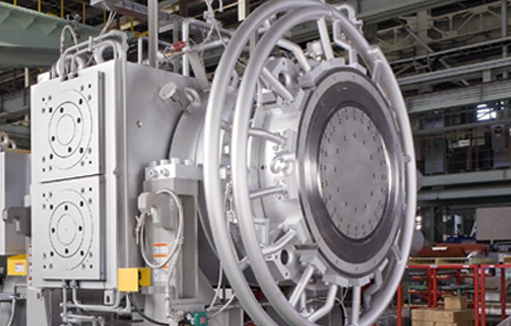
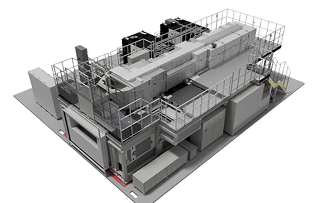
We have a broad lineup of equipment used in production of semiconductors, flat panel displays and other electronic components required for cutting-edge technologies such as 5G and automobile driving technology.
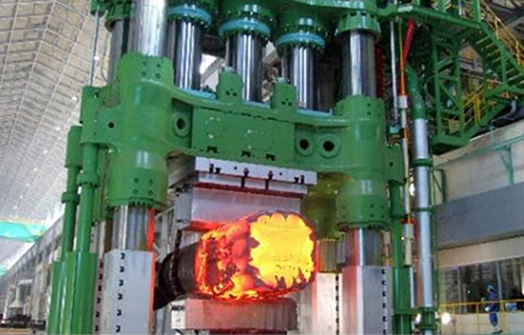
We also handle variety of products, which related to economic infrastructure and life culture, such as coupler/draft gear for rolling stock, food extruder and horse starting gate.
Products & Services
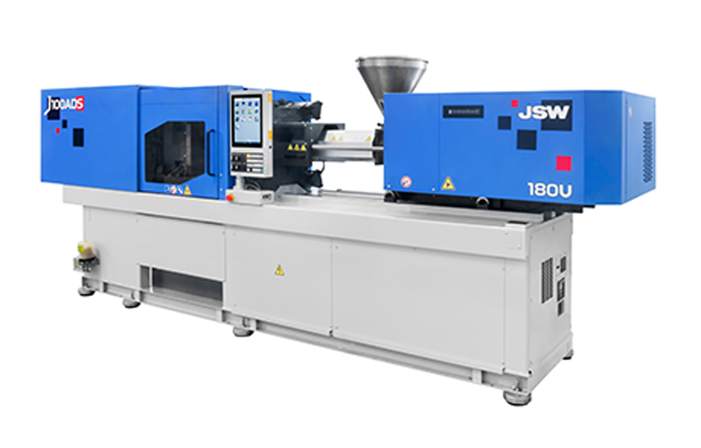
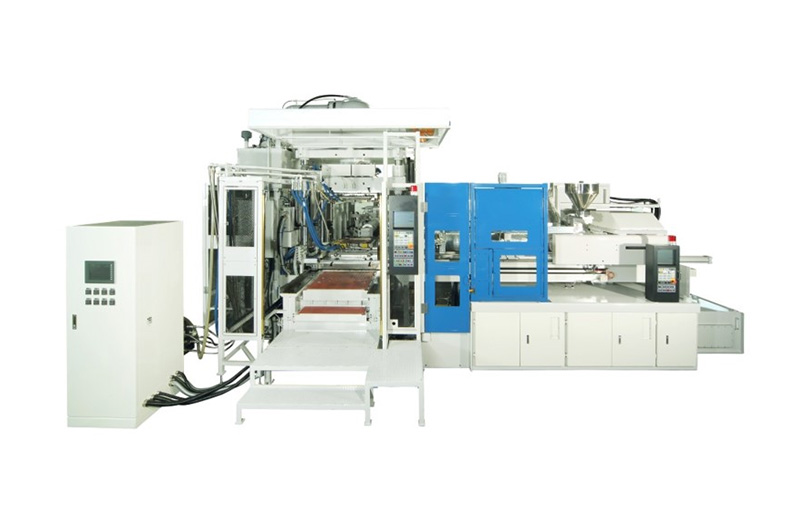
Electronic Device
-
$事業部門名$
$製品名$
$製品概要テキスト$$製品概要テキスト$$製品概要テキスト$$製品概要テキスト$$製品概要テキスト$$製品概要テキスト$
$タグ$
$タグ$$タグ$$タグ$
$タグ$$タグ$$タグ$
-
$事業部門名$
$製品名$
$製品概要テキスト$$製品概要テキスト$$製品概要テキスト$$製品概要テキスト$$製品概要テキスト$$製品概要テキスト$
$タグ$
$タグ$$タグ$$タグ$
-
$事業部門名$
$製品名$
$製品概要テキスト$$製品概要テキスト$$製品概要テキスト$$製品概要テキスト$$製品概要テキスト$$製品概要テキスト$
$タグ$
$タグ$$タグ$$タグ$
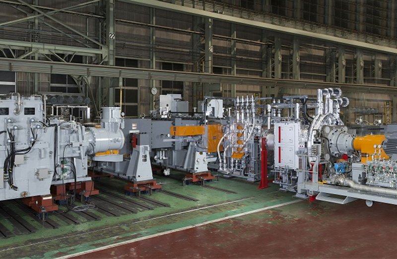
Economic Infrastructure
-
$事業部門名$
$製品名$
$製品概要テキスト$$製品概要テキスト$$製品概要テキスト$$製品概要テキスト$$製品概要テキスト$$製品概要テキスト$
$タグ$
$タグ$$タグ$$タグ$
$タグ$$タグ$$タグ$
-
$事業部門名$
$製品名$
$製品概要テキスト$$製品概要テキスト$$製品概要テキスト$$製品概要テキスト$$製品概要テキスト$$製品概要テキスト$
$タグ$
$タグ$$タグ$$タグ$
-
$事業部門名$
$製品名$
$製品概要テキスト$$製品概要テキスト$$製品概要テキスト$$製品概要テキスト$$製品概要テキスト$$製品概要テキスト$
$タグ$
$タグ$$タグ$$タグ$
Life & Culture
-
$事業部門名$
$製品名$
$製品概要テキスト$$製品概要テキスト$$製品概要テキスト$$製品概要テキスト$$製品概要テキスト$$製品概要テキスト$
$タグ$
$タグ$$タグ$$タグ$
$タグ$$タグ$$タグ$
-
$事業部門名$
$製品名$
$製品概要テキスト$$製品概要テキスト$$製品概要テキスト$$製品概要テキスト$$製品概要テキスト$$製品概要テキスト$
$タグ$
$タグ$$タグ$$タグ$
-
$事業部門名$
$製品名$
$製品概要テキスト$$製品概要テキスト$$製品概要テキスト$$製品概要テキスト$$製品概要テキスト$$製品概要テキスト$
$タグ$
$タグ$$タグ$$タグ$